High-efficiency Fabrication of 2μm Indium Micro-Bumps for Infrared Focal Plane Array Chips
Indium bump fabrication is a core process for high-density packaging of infrared focal plane arrays. Independent development of process equipment for indium bumps below 5 μm has become an urgent demand for the R&D and production of next-generation infrared devices.
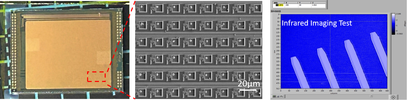
Shaoke Laser has conducted process tests on laser micro-bump printing and device interconnection verification for mass production of indium bumps ranging from 2 μm to 10 μm. The team realized laser-driven micro-droplet printing and packaging interconnection performance verification for infrared focal plane array chips featuring 2 μm bumps and a 640×512 array scale. The equipment has passed the on-site connectivity tests conducted by end users.
Compared with the conventional photolithography and evaporation process, the laser-driven micro-droplet printing technology boosts the production efficiency of indium bumps to 5,000 bumps per second. The total process steps are reduced from 9 to 2, and the production cycle is shortened from several days to just a few hours. This solution consolidates 9 sets of traditional semiconductor process equipment into a single unit. Mask-free laser direct writing enables flexible fabrication of indium bumps with diverse specifications. The technology effectively reduces the pitch of indium bumps and resolves the bottleneck of evaporation clogging in photolithographic holes for features below 5 μm. It represents the mainstream technical direction for the upgrade of next-generation ultra-high-density indium bump processes for infrared devices.